Freeze The Important Requirements First
Before drawing a symbol, record supply input, current demand, interfaces, connectors, board outline, mounting holes, environment, manufacturing constraints, and regulatory considerations. Identify high-voltage, high-current, radio-frequency, precision analog, and heat-producing sections. These facts determine layer count, spacing, copper weight, component choice, and physical separation.
Create a block diagram with power and signal flow. Mark connector direction and ownership so an input is not accidentally placed where an output is expected. If the design began as a microcontroller prototype, review every convenient development-board feature that the custom PCB must now provide, including regulation, reset, programming, clocking, and protection.
Capture Intent, Not Merely Connectivity
Organize the schematic by functional blocks and use clear net names. Include decoupling close to each device's supply pins, bulk capacitance where loads change, pull resistors, protection, test points, and programming access. Verify component ratings over the real voltage and temperature range. A part that works at nominal conditions may have too little margin during startup or a fault.
Check every symbol against the data sheet and every symbol-to-footprint assignment against the package drawing. Pin numbering mistakes and mirrored connectors are common because a schematic symbol, footprint, and physical component may be viewed from different sides. Print the footprint at actual size or compare it with a known part before ordering.
Run the electrical rules checker, but understand its limits. It can identify unconnected pins or conflicting types; it cannot know that two logically valid signals were swapped. Use a review checklist and have another person trace power, reset, clocks, communication, and connectors from source to destination.
Place Components By Current And Signal Flow
Lock the board outline, mounting holes, keep-out areas, and connectors first. Then place major functional blocks. Keep decoupling capacitors close to their pins with short return paths. Place crystals and sensitive analog components near the devices they serve. Keep switching power loops compact and separate noisy nodes from measurements.
Placement is where many routing problems should be solved. Rotate and move components until related pins face each other and critical paths are short. Leave room for assembly tools, probe access, heat spreading, and cable bend radius. A beautiful dense layout that cannot be inspected or repaired may be a poor prototype.
Route Critical Networks Deliberately
Define net classes for width, clearance, via size, and differential requirements before routing. Route power and critical signals first, then ordinary digital connections. Use a continuous reference plane where possible and avoid splitting the return path beneath fast signals. Keep high-current loops short and size copper for current and acceptable temperature rise.
High-speed interfaces require rules from the device and connector documentation. Length matching is not a decoration; it is useful only when skew limits require it. Likewise, 45-degree corners are less important than controlled impedance, reference continuity, coupling, and a valid stack-up. Coordinate impedance requirements with the fabricator.
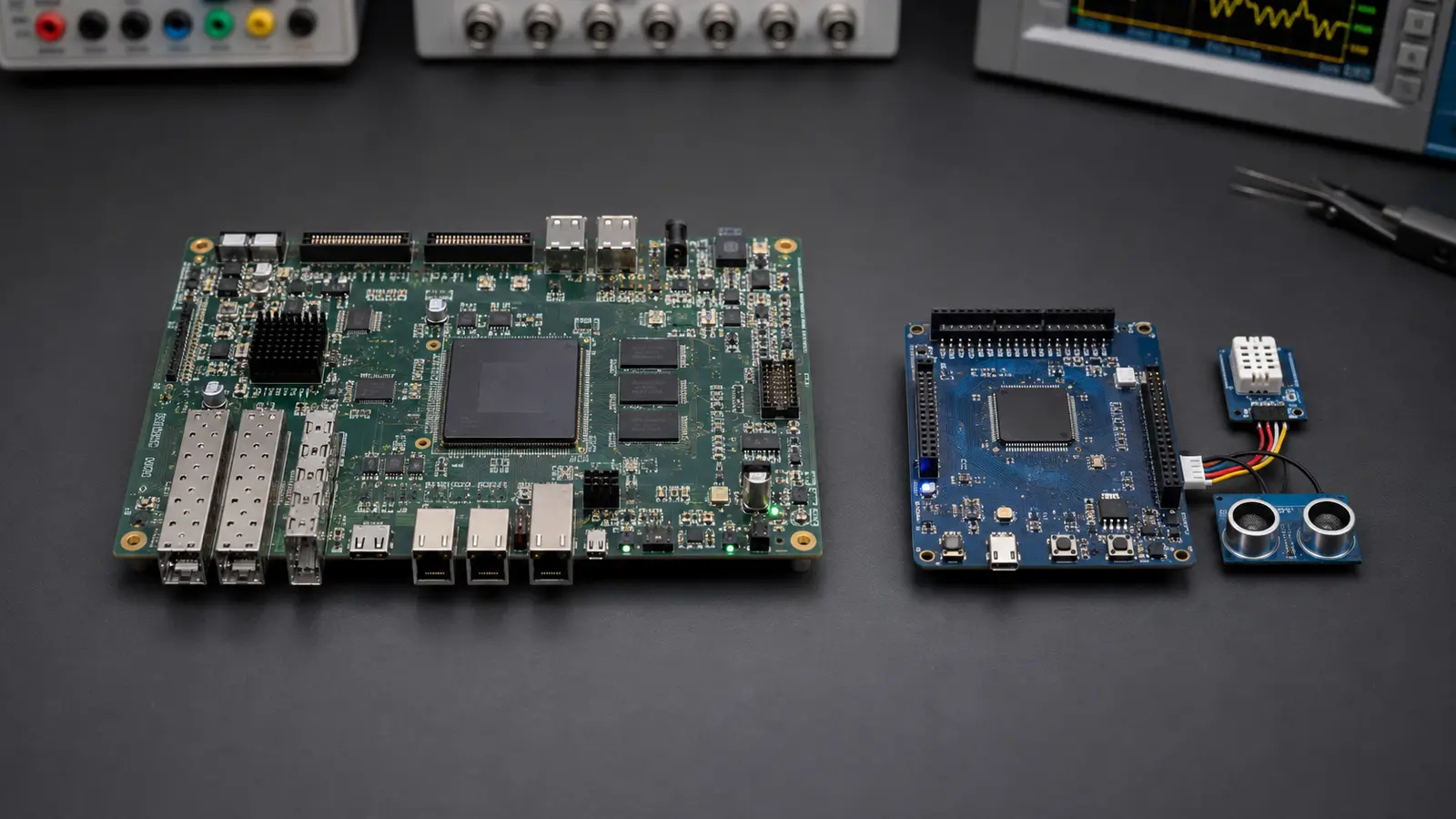
For mixed-signal boards, separate noisy and sensitive functions by placement and current flow rather than blindly cutting the ground plane. A broken plane can force return current around a long path. If the design contains dense parallel interfaces or large programmable logic, the FPGA decision should include package escape routing and layer cost.
Check The Design As A Manufacturer Will See It
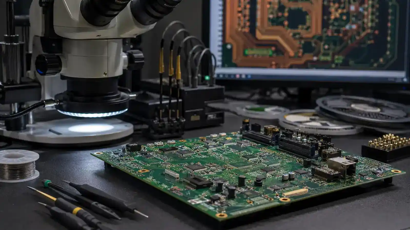
Run design-rule checks with the selected fabricator's capabilities. Inspect solder-mask openings, silkscreen, copper-to-edge spacing, annular rings, drill sizes, and component courtyard conflicts. Use the 3D view to catch connector orientation and mechanical collisions, but verify critical dimensions against drawings.
| Release item | Purpose | Review question |
|---|---|---|
| Gerber or fabrication data | Defines copper, mask, and legend | Are all intended layers present? |
| Drill files | Defines plated and non-plated holes | Do slots and mounting holes appear correctly? |
| Fabrication drawing | Communicates stack-up and notes | Are finish and tolerances explicit? |
| BOM | Identifies purchasable components | Are manufacturer part numbers complete? |
| Placement data | Locates assembled components | Does orientation match the assembly drawing? |
Open the exported manufacturing files in an independent viewer. This catches disabled layers, plotting mistakes, and assumptions hidden by the design tool. Archive the exact source revision, fabrication outputs, bill of materials, and assembly data together. Do not regenerate one file later without updating the release set.
Bring Up The First Board With Current Limits
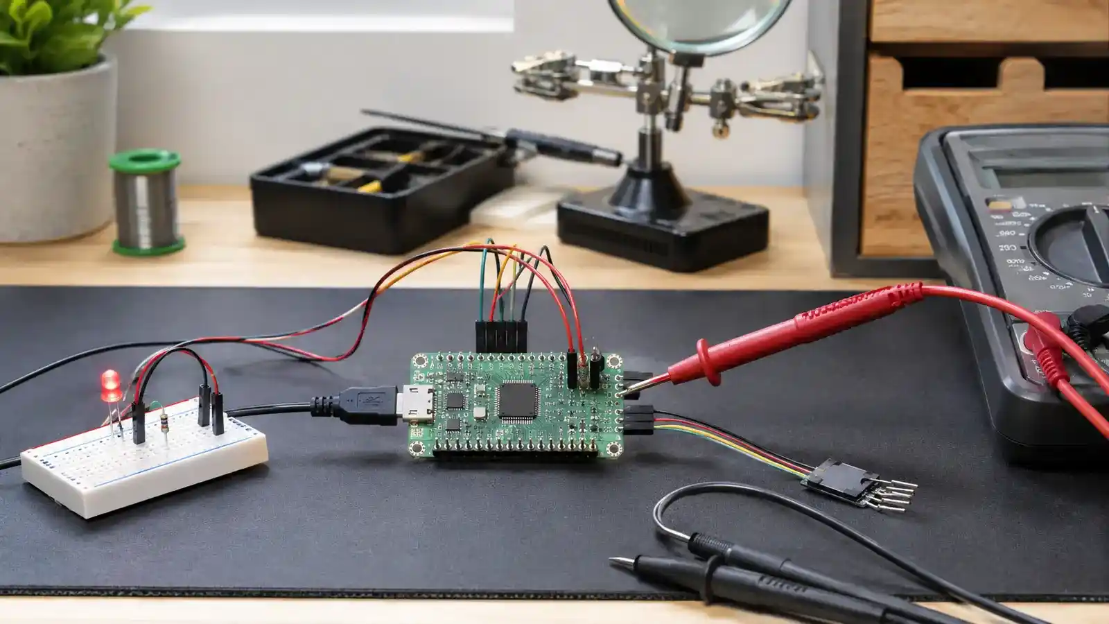
Inspect the unpowered board for polarity, solder bridges, missing parts, and damage. Measure resistance between power and ground, then apply power from a current-limited supply. Verify each rail before installing or enabling expensive loads. Check reset, clock, and programming access before testing the full application.
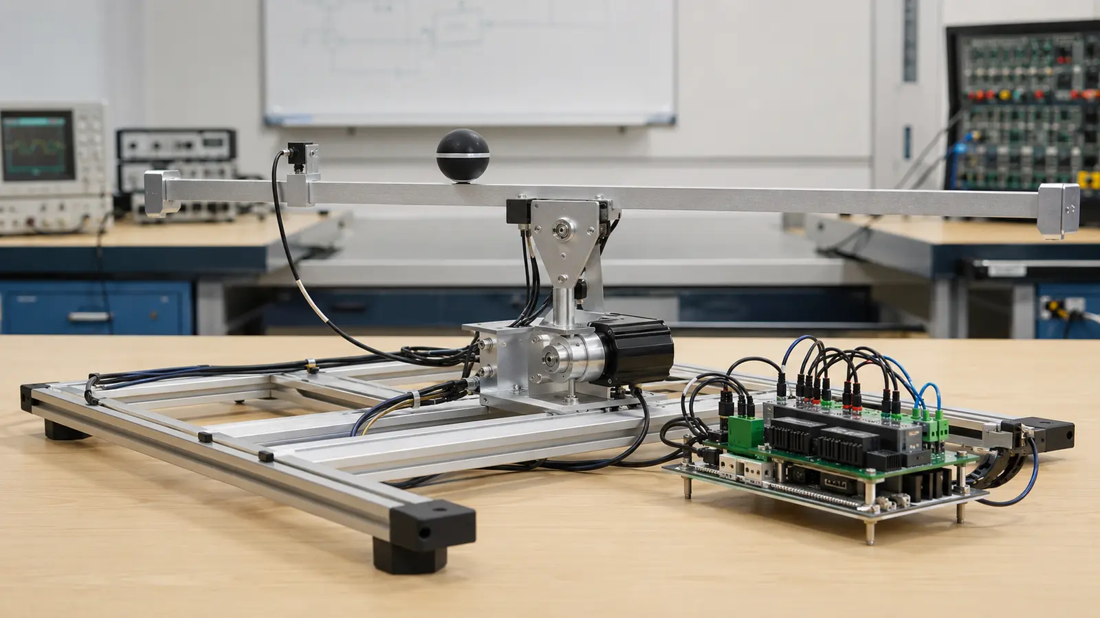
Use a structured test plan. Validate communication interfaces with known partners and expose critical timing on test points. Control projects should prove sensor and actuator directions before closing the loop; the PID control guide explains why an incorrect sign can immediately destabilize a mechanism.
Record every rework wire and component change. Update the schematic and layout rather than letting the physical prototype become the only accurate version. A successful first board is useful; an accurately documented second revision is a product-development asset.
Common PCB Workflow Questions
Should I Use Two Or Four Layers?
It depends on density, return paths, power distribution, impedance needs, and cost. Four layers often make continuous planes and routing easier, but a simple low-speed design can be valid on two when the return paths are deliberate.
Can Design Rules Guarantee The Board Works?
No. Rules verify geometric and some electrical constraints. They do not validate requirements, component choice, signal assignment, control behavior, or firmware.
When Should I Order A Small Prototype Run?
After independent review and manufacturing-file inspection, but before committing to volume. The prototype exists to expose electrical, mechanical, assembly, and test assumptions while changes remain affordable.